
Request Custom Lithium Niobate Wafers
Specify the crystal orientation, dimensions, thickness, surface finish and any doping requirements for your custom lithium niobate (LiNbO₃) substrates. Request availability and a quote for photonics, surface acoustic wave (SAW) devices or sensing research.
Get Your Custom LiNbO₃ Wafer Quote FAST! Or, Buy Online and Start Researching Today!.
LiNbO₃ Wafer Applications and Specifications
Lithium Niobate (LiNbO₃) is a versatile material for optical modulators, SAW devices, nonlinear optics and sensing. A custom lithium niobate substrate can be specified by crystal cut, thickness, diameter and polishing requirements to suit the intended fabrication process. Thin-film LiNbO₃-on-insulator (LNOI) is a related platform for integrated photonic circuits.
Core Properties
LiNbO₃ is transparent from ~350–5200 nm with a high refractive index (> 2.3) and strong birefringence. Its large electro-optic coefficients (r33 ≈ 30 pm/V) enable ultrafast modulation, while significant nonlinear coefficients support frequency conversion (e.g., SHG). It is also ferroelectric with a high Curie temperature (~1140 °C).
Orientation Matters
Because LiNbO₃ is anisotropic, the crystal cut and propagation direction affect electro-optic and acoustic device behavior. X-cut and Z-cut are both used in optical devices depending on waveguide design and electrode geometry; rotated Y-cuts, including 128° Y-X, are common in SAW research. Specify the cut and orientation tolerance needed for your process when requesting a quote.
Dimensions & Finishing
Lithium niobate is available in wafer and diced-piece formats, with size, thickness, bow, warp and orientation tolerance specified for the application. Single-side polished (SSP) and double-side polished (DSP) finishes can be requested; confirm achievable dimensions, surface quality and tolerances for the selected grade and cut.
Advanced Platforms & Doping
Thin-film lithium niobate on insulator (LNOI) places a submicrometer LiNbO₃ layer on SiO₂/handle, enabling high-index-contrast waveguides and compact PICs. Periodically poled LiNbO₃ (PPLN) can provide quasi-phase matching for nonlinear optical conversion; the poling period depends on wavelength, temperature and device design. Dopants have different roles: MgO can improve resistance to photorefractive damage, while Fe is used to enhance photorefractive behavior. Confirm dopant composition and availability for the intended wafer.
Applications Snapshot
Customized LiNbO₃ underpins telecommunications (EO modulators, waveguides), RF/acoustic systems (SAW filters/resonators), and sensing. Emerging areas include quantum information, integrated photonics, and biomedical platforms (e.g., lab-on-a-chip, label-free biosensors, acoustic tweezers).
Manufacturing & Quality Assurance
Production includes Czochralski growth, precision slicing/grinding, and optical polishing. QA covers XRD for orientation, interferometry for flatness, AFM/profilometry for roughness, and optical inspection—delivering traceable reports per wafer/batch.
From Spec to Substrate
A practical ordering flow defines orientation (standard or custom angle), dimensions and thickness, surface finish (SSP/DSP/roughness), tolerances, and any special requirements (coatings, patterning, poling). Quotation → confirmation → fabrication proceeds with ongoing communication and packaging for optical-grade materials.
Built for Research
For R&D, small-quantity orders and sample kits support comparative studies across cuts and finishes, with rapid delivery and technical consultation to help map application goals to material parameters and accelerate iteration.
As integrated photonics grows alongside electronics, the demand for precisely specified LiNbO₃ continues to rise—especially with LNOI bridging high performance and chip-scale integration for next-generation devices.
Why LiNbO₃ Remains Foundational
Lithium Niobate (LiNbO₃) substrates bridge the gap between optical, electronic, and acoustic domains. Their combination of transparency, strong electro-optic response, and piezoelectric coupling makes them indispensable for devices that modulate, convert, or sense signals across light and sound.
As industries move toward integrated photonics, LiNbO₃’s ability to merge photonic and electronic functions on one substrate supports faster, energy-efficient systems—from telecom modulators to next-generation sensors.
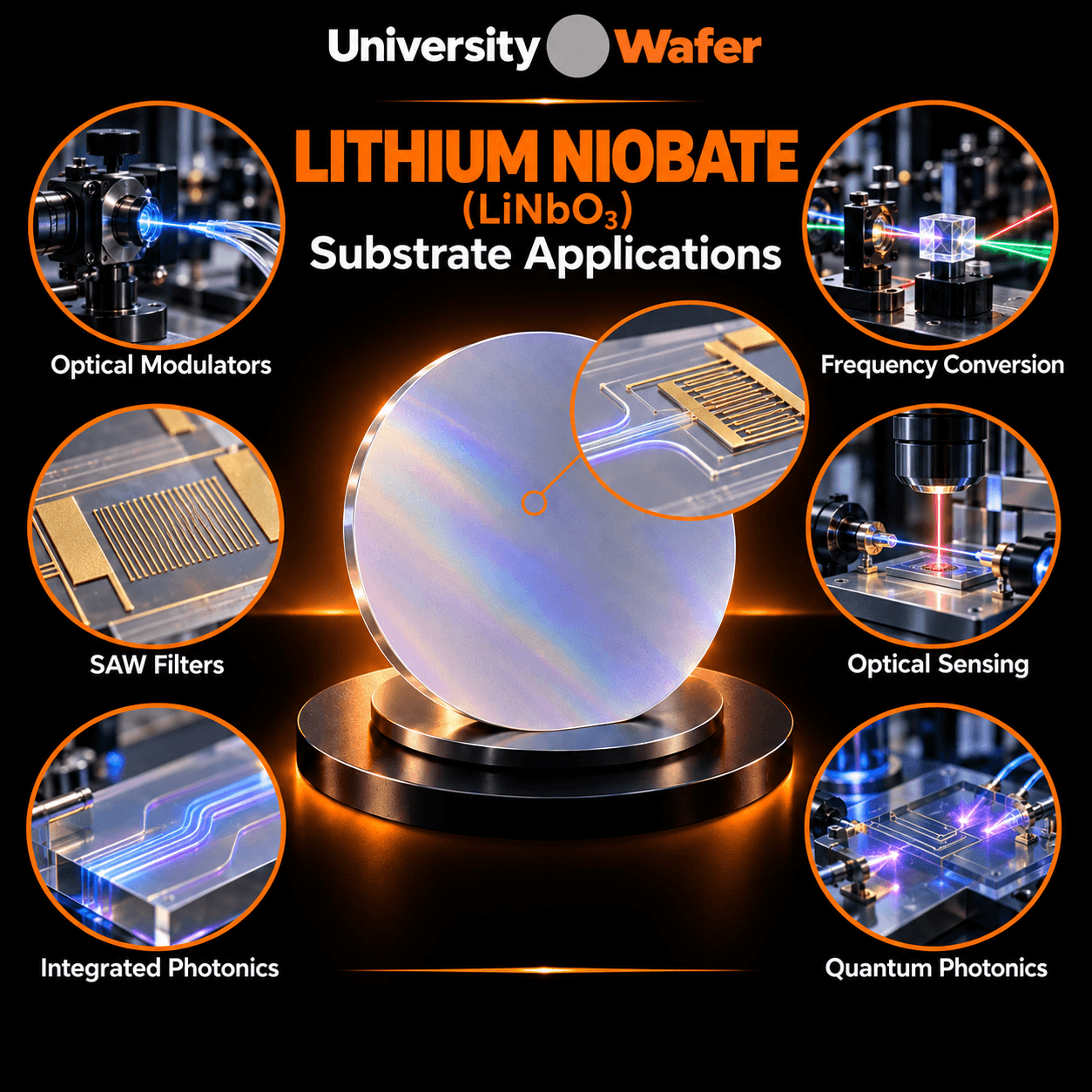
Material Versatility
The same LiNbO₃ wafer can serve radically different purposes based on its crystallographic orientation. Z-cut substrates optimize electro-optic modulation, Y128°-cut substrates excel in surface acoustic wave (SAW) applications, and doped variants extend optical-damage thresholds for high-power systems. This flexibility enables tailored performance across research and manufacturing.
Advanced thin-film LNOI (Lithium Niobate on Insulator) adds another layer of capability—allowing chip-scale photonics with the same high optical quality that defines bulk LiNbO₃ wafers.
Applications Driving Demand
Customized LiNbO₃ substrates underpin a wide spectrum of technologies: telecommunications, quantum optics, biomedical sensing, and integrated photonic circuits. Researchers use them to fabricate modulators, frequency converters, biosensors, and terahertz devices—each benefiting from LiNbO₃’s stable, controllable response to electric and optical stimuli.
In biomedical fields, LiNbO₃ enables label-free biosensors, lab-on-a-chip diagnostics, and even acoustic tweezers for cell manipulation—all leveraging the material’s acoustic precision and biocompatibility.
Precision Through Customization
Every specification—orientation, polish, dopant level, or thickness—directly influences how a device performs. Precision control ensures phase-matched nonlinear optics, stable SAW propagation, and high-efficiency modulation. Customization isn’t aesthetic—it’s functional engineering that defines how your system interacts with light, sound, and electricity.
Research Impact
As photonic integration grows alongside electronics, researchers rely on UniversityWafer’s customized LiNbO₃ wafers to prototype next-generation components. From small-scale optical test structures to production-grade devices, these substrates provide reproducibility, orientation accuracy, and quality assurance that accelerate innovation across disciplines.
Key Facts — LiNbO₃
- Combines electro-optic, nonlinear, piezoelectric & ferroelectric properties.
- Wide transparency (~350–5200 nm), high index (n ≳ 2.2–2.3), low loss optics.
- Its electro-optic response supports modulators; achievable bandwidth depends on device design, not the substrate alone.
- Ferroelectric with high Curie temperature (~1140 °C).
Cuts & Orientations
- X-cut / Y-cut / Z-cut: select by device geometry, optical polarization and/or acoustic propagation direction.
- Angle cuts: 36°Y-X, 64°Y-X, 128°Y-X for RF/SAW performance & stability.
- Specify custom-cut orientation and request an X-ray orientation measurement or tolerance with the quote.
Size & Thickness
- Diameters: 1″–4″+ (research samples to production wafers).
- Thickness and tolerances depend on the cut, size and finish; confirm by quotation.
- Bow/warp control & custom shapes (rectangles/squares) on request.
Surface Quality
- SSP or DSP polish; request the roughness specification needed for your process.
- Specify scratch-dig, flatness and inspection requirements when requesting a quote.
- Patterned/activated surfaces for bonding & alignment features.
Doping & Material Mods
- MgO doping can improve resistance to photorefractive damage; specify the required composition.
- Fe doping enhances photorefractive response; ask about other available compositions for specific research needs.
- Rare-earth options for active media; Li/Nb ratio tuning available.
Thin-Film LNOI
- Enables compact, low-power PICs, tight confinement, small bend radii.
- Ideal for modulators, frequency converters, and integrated quantum optics.
Applications (Where It Fits)
- Telecom & Photonics: modulators, waveguides, switches, frequency conversion.
- RF & Acoustic: SAW filters, delay lines, resonators (high K² cuts for wide bandwidth).
- Sensing & Measurement: bio/chemical, pressure/temperature, structural health.
- Quantum/Integrated: SPDC sources, QKD, PICs, frequency combs, neuromorphic photonics.
Manufacturing & QA
- Czochralski growth; precision slicing, grinding, and optical polishing.
- Available characterization may include XRD orientation, flatness, roughness and optical inspection; request the measurements required for your order.
- Traceable reports available per wafer/batch.
Related Lithium Niobate Resources
- Lithium niobate (LiNbO₃) wafers — cuts, grades, and research requests.
- Lithium niobate on insulator (LNOI) — thin-film substrates for integrated photonics.
- LiNbO₃ substrates for SAW devices — acoustic applications and cut selection.
- LiNbO₃ wafers for optical modulators — bulk and thin-film device platforms.
- Optical-grade LiNbO₃ wafers — choosing a suitable surface finish.
- LiNbO₃ for nonlinear optics — frequency-conversion research.