
Wafers for Avalanche Transit Time Diode Research
A research client asked for the following:
We are presently doing research in the field of high-power RF Avalanche Transit Time diode development. For that we need to purchase GaN epiwafer on Si or SiC or Sapphire or GaN substrates. Please share the comparative price list so that the final order could be placed based on this. Tentative Specification: p+ (cap layer) : 5x10^25 / m^3 , 50 nm n+ : 1x10^26 / m^3 , 5 micron n layer : 5x10^23/m^3, 1 micron p-layer: 5x10^23/m^3 , 1 micron Substrate (n type) : Si, GaN, SiC and Sapphire : quote separately Please quote for unit processed epiwafer ( wafer dia, 4 inch / 6 inch / as per availability at your centre). Please make a table of all added details as you feel appropriate for fabrication team. In quotation, please mention, whether there is any condition of minumum number of purchase - accordingly , the final order would be placed.
Substrate and epitaxial options to compare for this research include GaN on silicon, GaN on silicon carbide, GaN on sapphire, and bulk GaN substrates. Related material options include silicon carbide (SiC) and silicon wafers. Device-ready layer structures and availability depend on the requested specification.
Get Your RF Semiconductor Wafer Quote FAST! Or, Buy Online and Start Researching Today!
What Is an IMPATT Diode?
An IMPATT diode (impact-ionization avalanche transit-time diode) is a reverse-biased semiconductor device investigated as a microwave oscillator and amplifier. When the junction operates in avalanche breakdown, impact ionization generates electron-hole pairs. The delay from avalanche buildup and carrier travel through a drift region can produce negative resistance at microwave frequencies when the device and circuit are designed for that operating range.

How Avalanche Transit-Time Operation Works
An IMPATT structure includes an avalanche region and a drift region. The reverse electric field initiates impact ionization, and the generated carriers move across the drift region. Their transit time contributes to the phase shift between RF voltage and current. Device geometry, doping, heat removal, and the surrounding resonant circuit influence operating frequency, output power, efficiency, and noise.
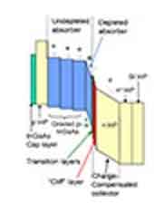 IMPATT and TRAPATT are distinct avalanche transit-time device concepts. TRAPATT (trapped plasma avalanche triggered transit) operation involves a traveling avalanche and a dense carrier plasma. Neither mechanism should be confused with a Gunn diode, which relies on a different negative-resistance effect. Researchers considering these devices can review p-n junctions and epitaxial silicon wafers alongside the intended diode architecture.
Wafer Materials for RF Avalanche Diode Research
Silicon wafers are a research platform for avalanche diode structures. Wide-bandgap materials such as gallium nitride (GaN) and silicon carbide (SiC) are also studied for high-field and high-power devices. For GaN epitaxy, substrate choices include GaN on silicon, GaN on SiC, GaN on sapphire, and native GaN. Each option has different thermal, electrical, and fabrication tradeoffs; a standard RF transistor epiwafer is not automatically suitable for an avalanche transit-time diode.
For a quote, specify substrate material, diameter, orientation, doping profile and concentrations, epitaxial layer thicknesses, polarity, surface finish, quantity, and the intended device structure. These details determine which research wafer or custom epitaxial stack may be appropriate.